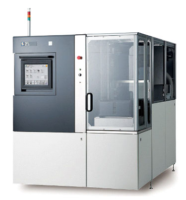
⦁ ProPowertek utilizes laser cutting equipment from the internationally renowned DISCO Corporation, offering a variety of cutting services including Laser Dicing and Laser Grooving. Combined with Blade Dicing, these methods provide flexible wafer dicing solutions suitable for thick metals, high-hardness materials, and third-generation compound semiconductor products.
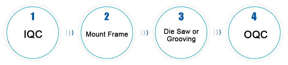
▶ All wafer dicing (Die Saw) processes utilize a full suite of fully automated DISCO equipment. We possess both blade dicing and laser cutting machines, with the laser systems providing dicing and laser grooving services. ▶ We flexibly address challenges encountered with different materials during the cutting process, offering various combinations such as Blade Dicing (BD), Laser Dicing (LD), Laser Grooving (LG), Laser Grooving (LG) + Blade Dicing (BD), and Blade Dicing (BD) + Laser Dicing (LD). ▶ ProPowertek is equipped with Automatic Optical Inspection (AOI) systems to provide post-dicing die inspection services. Combined with CP wafer testing, we generate a comprehensive wafer map to assist downstream packaging in selecting good dies.
Case Sharing
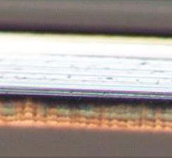
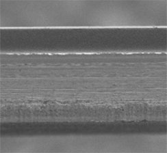
Backside copper (Cu) metal silicon wafers processed using blade dicing first, followed by laser dicing.
OM Image (side-wall inspection)
SEM Image (side-wall inspection)
Application
⏺︎ Standard wafer dicing, multi-project wafer (MPW) dicing, GaN on Si dicing, laser grooving, and thick metal dicing.