“After passing the WAT (Wafer Acceptance Test) in the front end wafer foundry. How to handle the wafer thinning and back side metallization before assembly?“
“Finally wafer thinning and back side metallization were finished, but you need to transport wafer to another suppliers for CP and sawing with high risk, is there any place to do it right one time?“
ProPowertek has recruited professional experts and implement advanced processing to assist you in completing wafer thinning and back side metallization in short time.
⏺︎ Various solutions for surface grinding process ⏺︎ Various solutions for backside metallization ⏺︎ Backside silver thickness to 15um (even can be customized up to 40um) and various solutions for front side metallization ⏺︎ A complete and extensive one-stop service
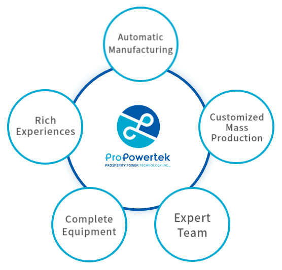
Service Features
⏺︎ One-Stop Service
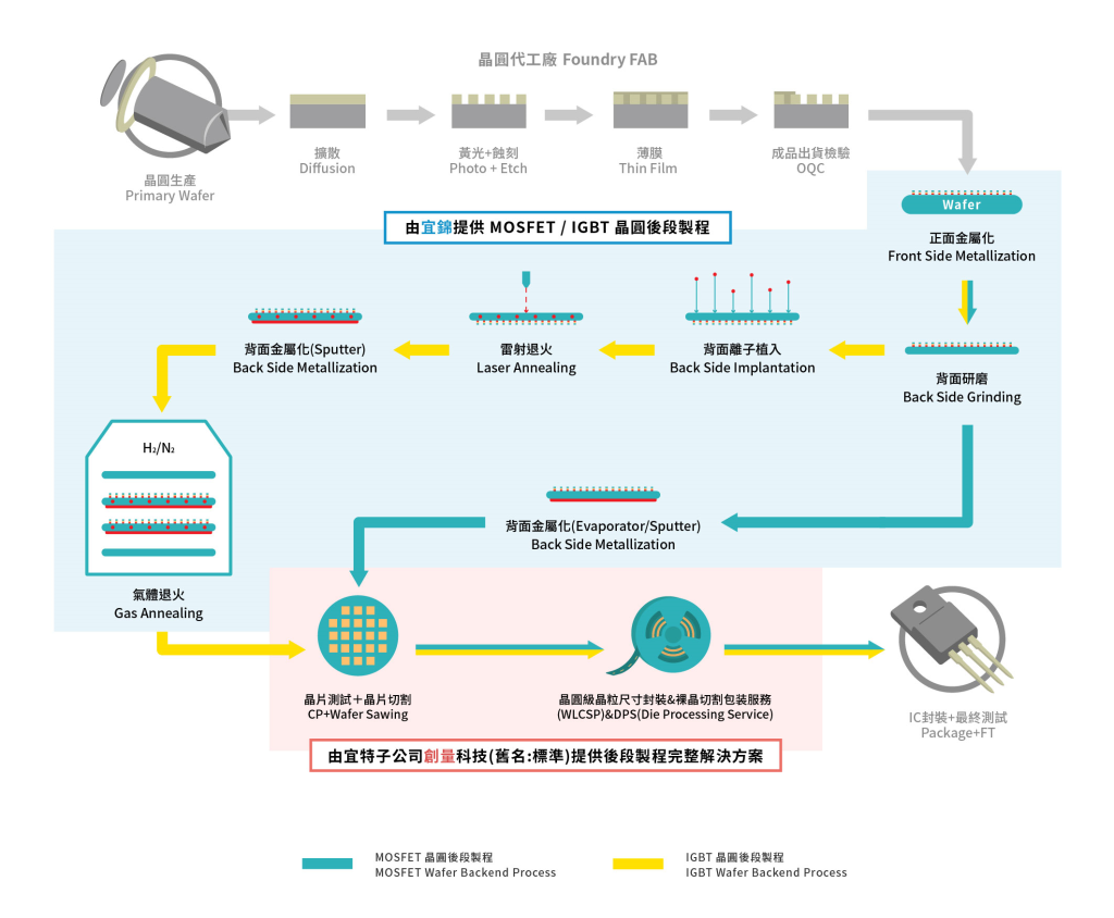
Front Side Metallization Process
Front Side Metallization Process
Back Side Grinding Process
Back Side Grinding Process
Back Side Metallization Process
Back Side Metallization Process
IGBT Wafer Backend Process
IGBT Wafer Backend Process
⏺︎ Other Services
Turnkey Solution for Backend Process
Turnkey Solution for Backend Process
Semiconductor Manufacturing Process
ProPowertek is capable to provide one-stop MOSFET backend solution including WLCSP, CP and DPS in cooperation with its subsidiary, ITS (see the blue and pink highlight for ProPowertek & ITS services).